Week 04: Electronics Production

PCB - Printed Circuit Board"
 We have learned that a PCB is a printed circuit board. This means that traces are printed on insulated material. The utilized boards consist of different layers of material. One layer is made of conductive copper, and another layer is made of insulating material. To print traces on the boards, copper lines are isolated by milling away the surrounding material. Components such as LEDs, resistors, switches, etc., can be attached to these traces. PCBs are present in almost all technical devices (smartphones, computers, household appliances, etc.). A PCB can be designed differently to meet the requirements of the device. There are also boards that can be printed on both sides, which helps save space in even smaller technical devices.
Manufacturing the PCB
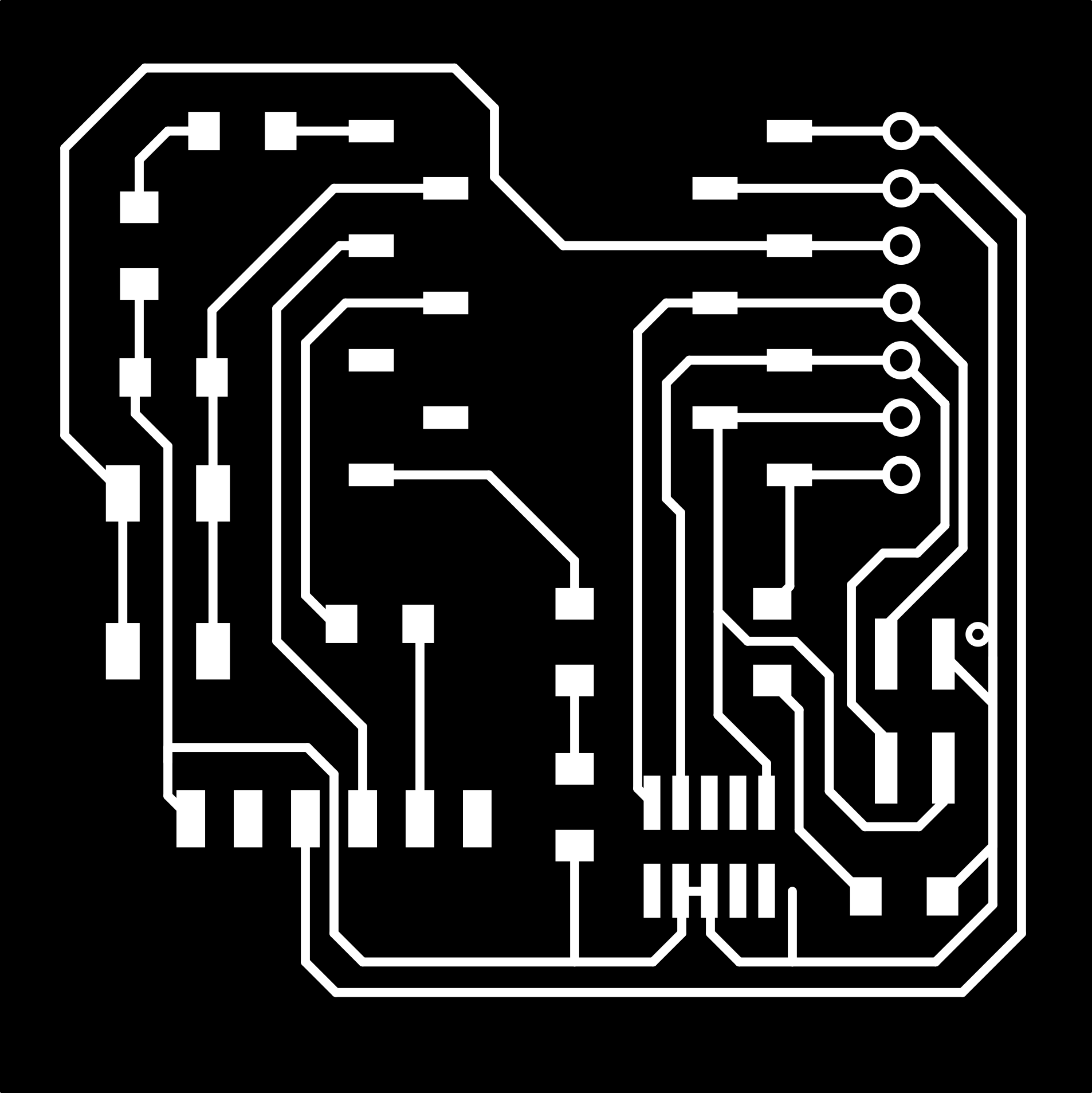 To print the circuit board, we needed to get ready-made images into the correct format for the milling machine. For this purpose, we downloaded three images showing all the components to be printed. The first image contained the traces, the second image the holes, and the third image the outlines.
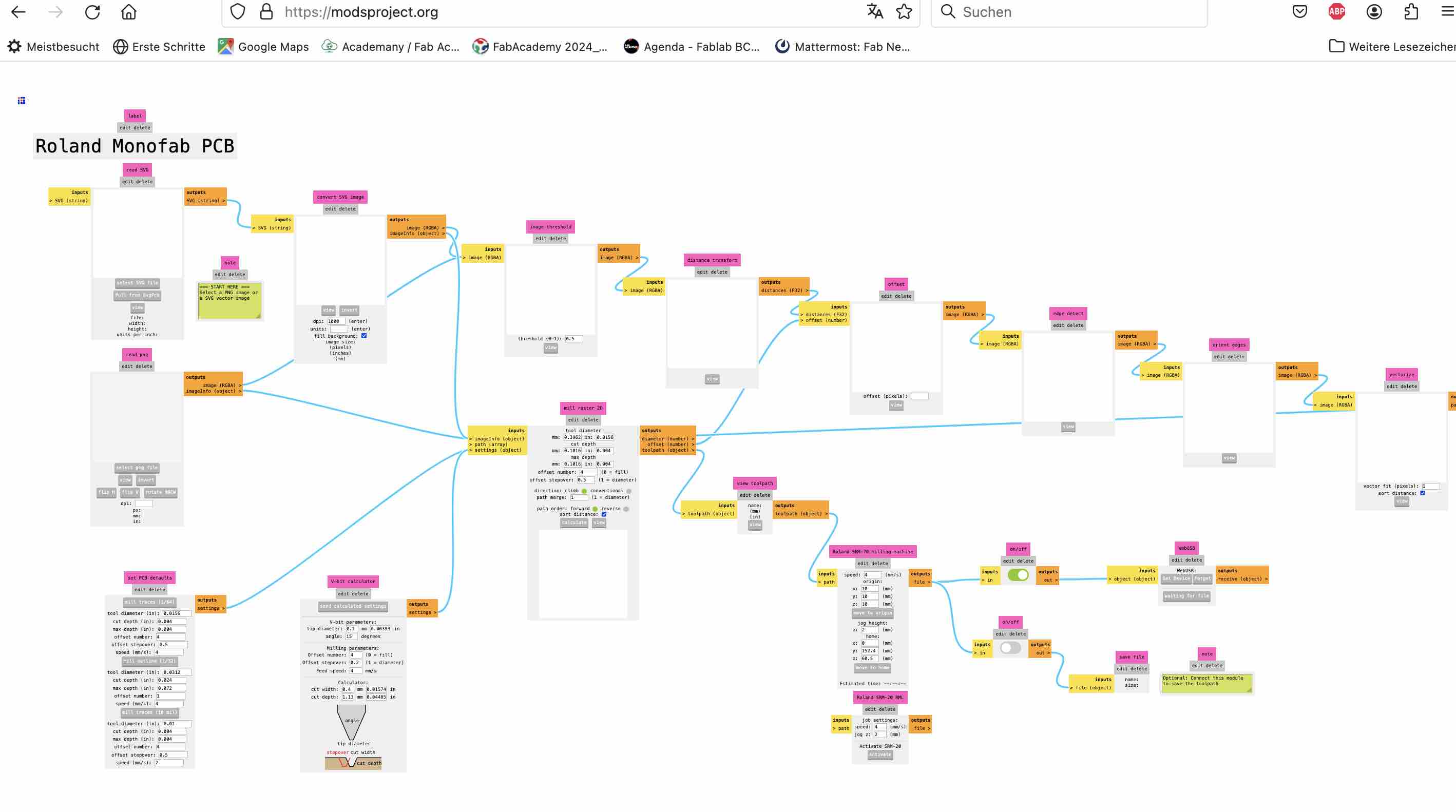 We uploaded the images one by one to a platform designated for this purpose. The printing process occurs in the order described above. It's essential to start each printing job individually, and each type of print (traces, holes, or outline) requires different settings. Once all settings are configured, I had to select "calculate," and the download started automatically. With the "view" option, I could check if everything looked good.
Stettings for traces
- mill traces: 1/64
- Smill traces: 1/64
- Offset Number: recommended 4 (if you put 0, then everything will be lined out)
- Speed: 3 mm/s
- origin: x, y, z = 0
- job high: 5 mm
- home: z always unequal to 0
- edit delete: on
Settings for holes and outlines
- mill traces: 1/32
- mill traces: 1/32
- max depth: 1.75
- Speed: 1.5 mm/s (hole) and 0.5 mm/s (outline)
- origin: x, y, z = 0
- job high: 5 mm
- home: z always unequal to 0
- edit delete: on
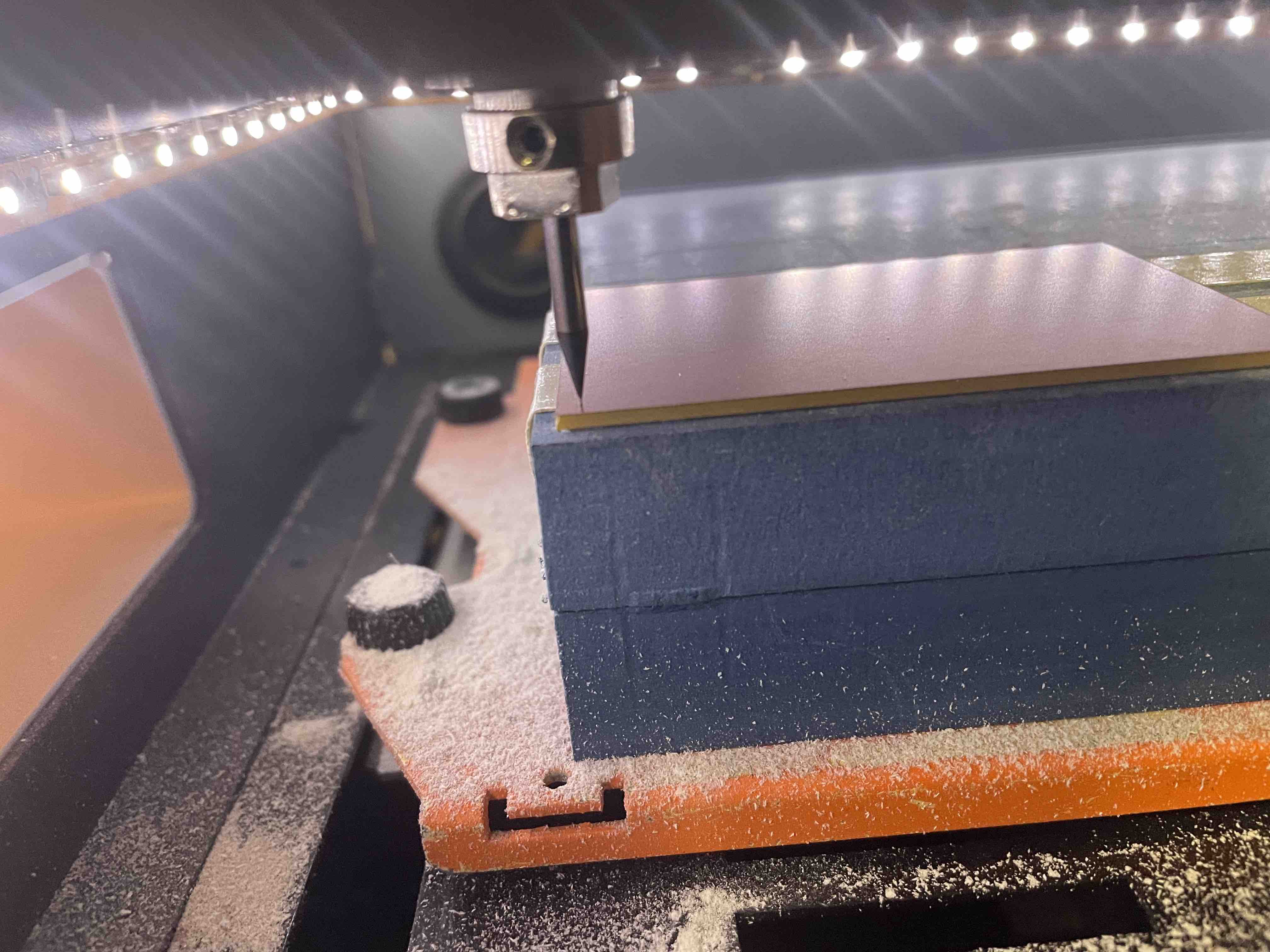 It's crucial that the board is flatly placed and glued in the laser printer. After that, the cutter needs to be positioned. The cutter is navigated to the left front corner. The x and z zero point can be easily set. For the y zero point, the cutter is navigated as near as possible towards the material. Then the screw is opened again so that the cutter is precisely on the material, then the screw is closed again. This is now the x/y/z zero point can be record in the program. Now the cutter is navigated slightly upwards, and the print is started.
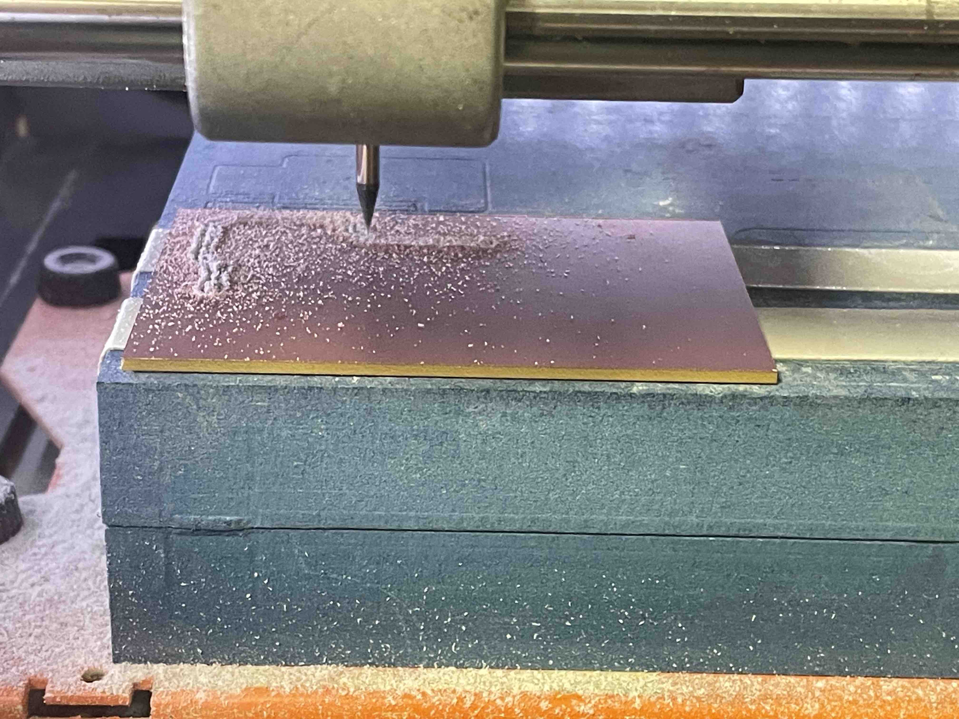 But then, after starting the first print of my traces, I noticed a mistake. I also changed the maximum depth in case of the traces, and it went really too deep. I had to download the file again after changing the maximum depth to 0.1016. After waiting until it finished, I could see that some traces were good, and others were not deep enough. I could use the same PCB again, but I had to start a third round of milling after making the y-axis 0 a bit deeper.
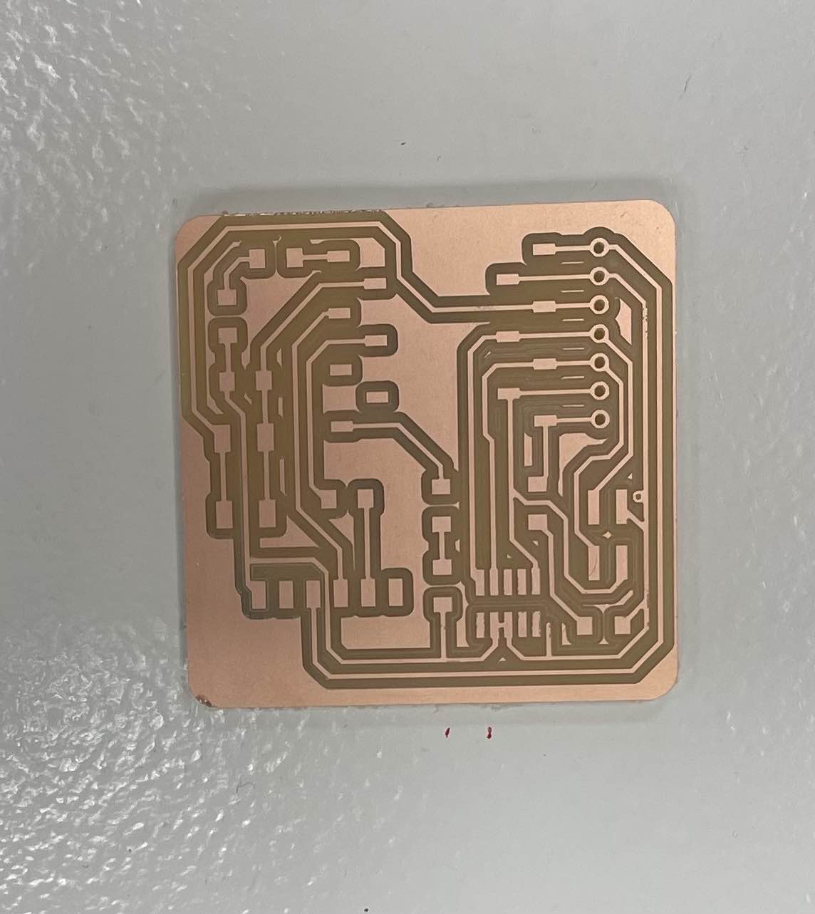 Finally, everything went well, and I could continue with the holes and the outline. I was really glad to hold my first self-made PCB in my hand.
Group assignment
On this page, you will find all the information regarding to our group assignment.
Soldering
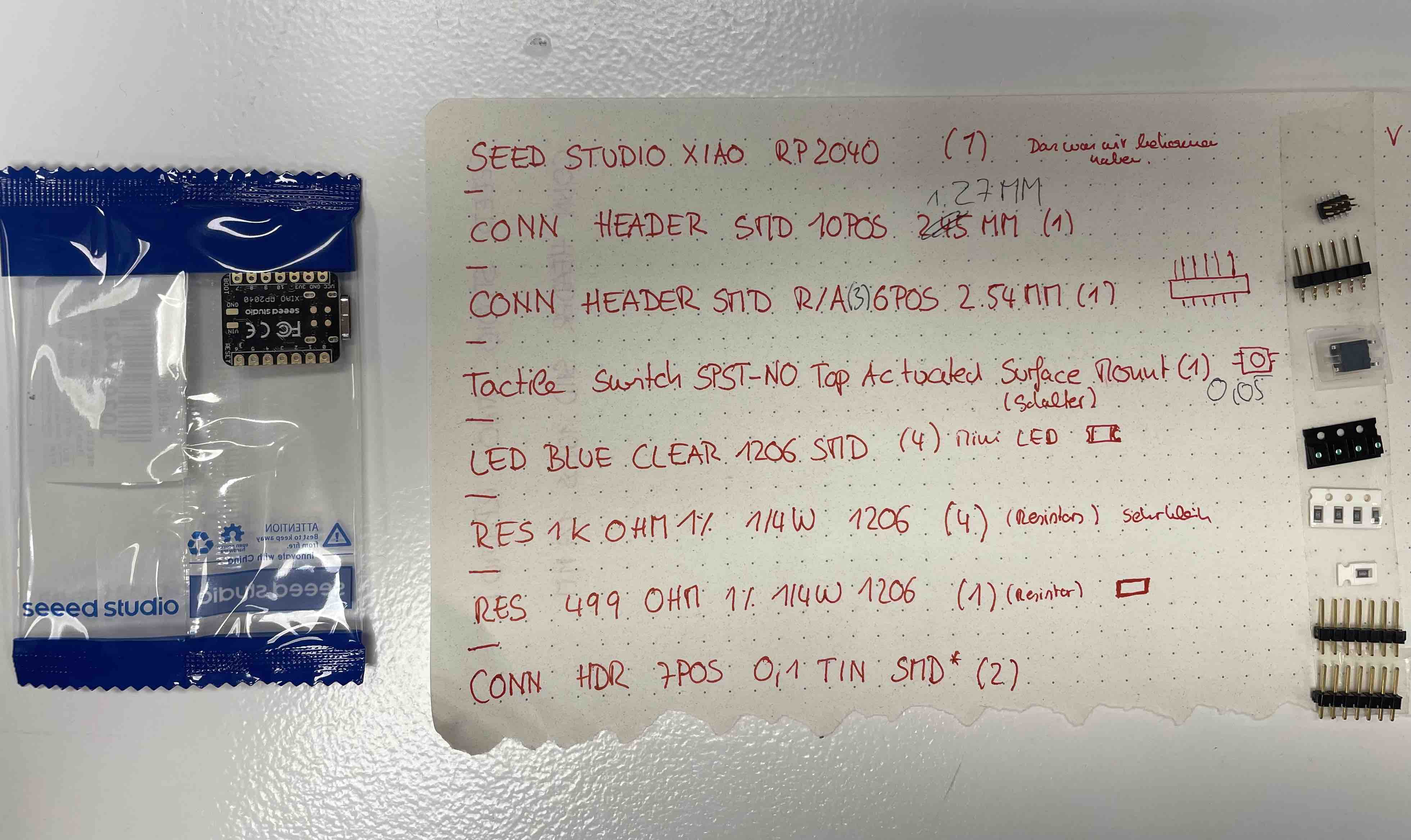 AFirst, I had to gather all the components I needed for the circuit board. Once I found them all, I started soldering.
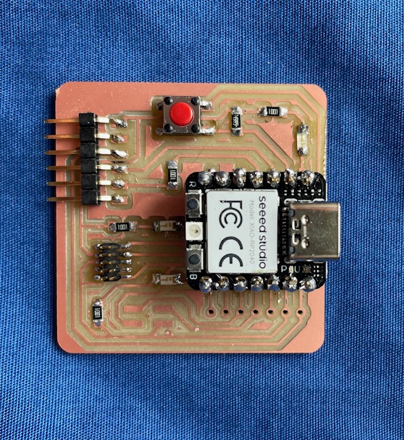 I hadn't soldered before, but it was easier than I thought. From my perspective, this was mainly because smaller mistakes can be corrected well by reheating and using solder wick. However, it still took some time to attach all the components.
First programming
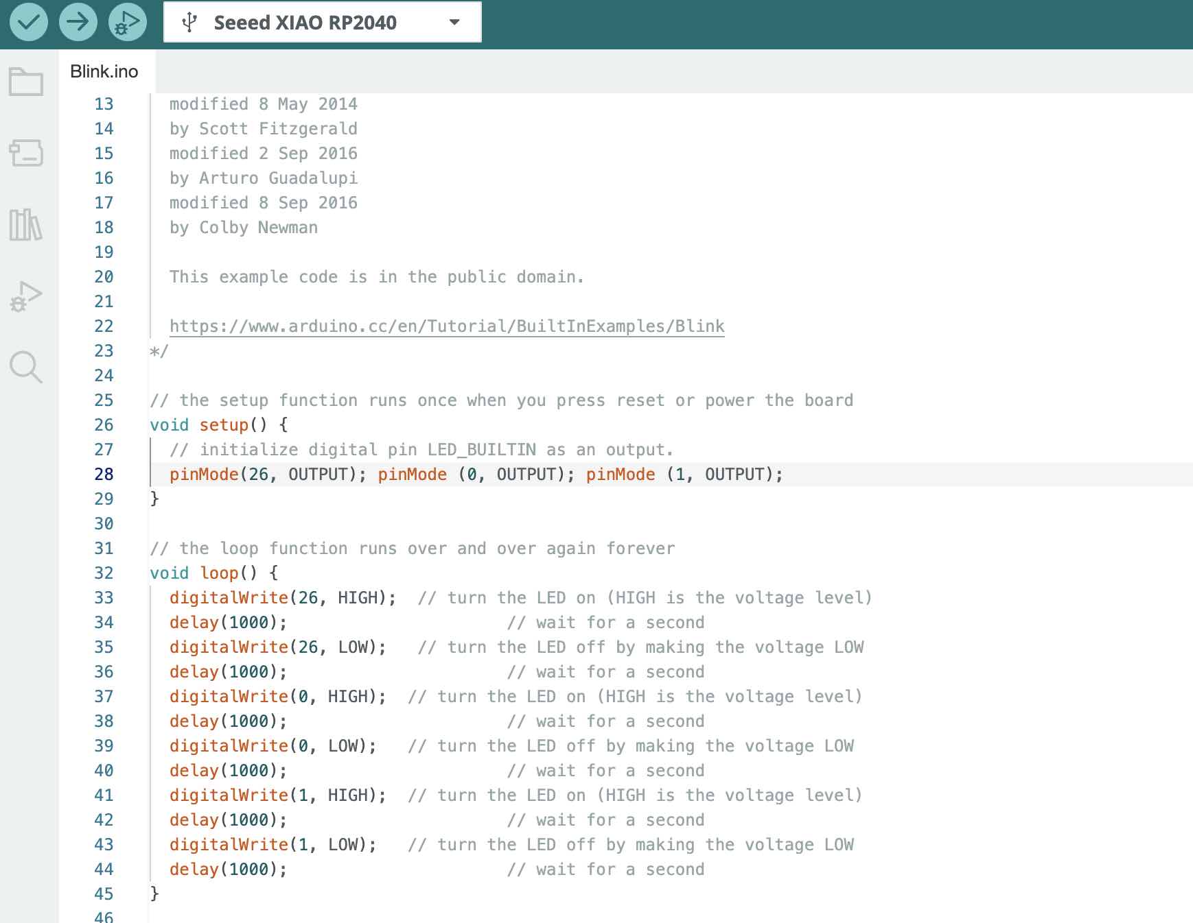
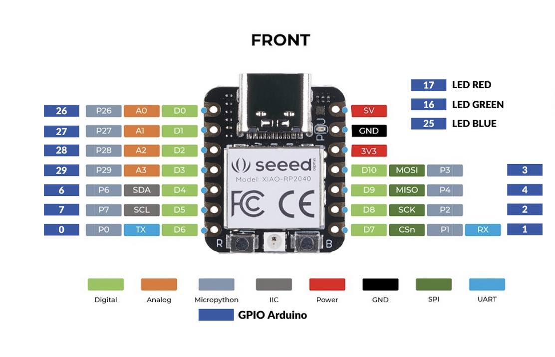
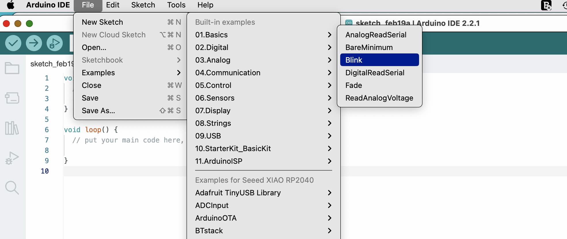 AI initially measured with a multimeter to check if the connections were functioning. When everything seemed to be fine, I connected the PCB to my computer and opened Arduino. First, I had to expand Arduino to work with additional boards. Then, I searched for and added the XIAO board in the Boards Manager. Next, I worked with two examples. Firstly, under File > Examples > 01.Basics > Blink, I opened the Blink option. I then looked online to find out which numbers corresponded to the outputs of the PCB and which LEDs they were connected to. Afterwards, I adjusted the code and loaded it onto the PCB. All lights blinked one after the other.